 +86 183 6377 3366

0102030405
Glass substrate, strong momentum!
2025-09-19
As a packaging substrate, the advantages of Glass are very obvious. It is very flat and has lower thermal expansion than organic substrates, thus simplifying the lithography process.
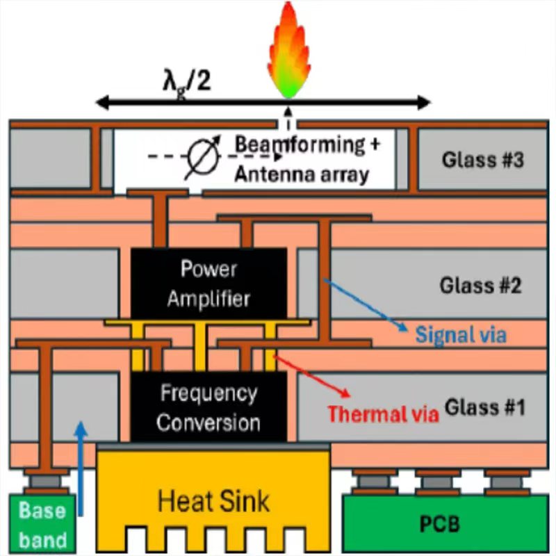
This is just the beginning. The growing warping problem of multi-chip packaging has been significantly improved. The chips can be mixed bonded to the redistribution pad on the glass. Moreover, compared with the movement substrate, the glass substrate provides extremely low transmission losses for high-frequency and high-speed devices.
Worse, silicon interposers and movement substrates are also losing momentum to develop. Glass is much cheaper than silicon interposers, with a 50% reduction in warpage and a 35% improvement in position accuracy. This makes it easier to achieve redistribution layers (RDLs) with line widths and spacings less than 2 microns, which is difficult for the movement substrates. Furthermore, the transparency of the glass at communication wavelengths enables the waveguide to be embedded in a stacked glass structure for 6G applications. Ultra-thin (less than 100 microns) glass is easily made into large sizes of 700 x 700 mm.
Glass (usually borosilicate glass or quartz glass) is also very flexible in its use. It can be used as a carrier, core substrate for embedded components, 3D stacking material, or as a sealed cavity for sensors and MEMS. Glass has better conductivity than organics and therefore can more effectively conduct heat from active devices. Its coefficient of thermal expansion (CTE) can be adjusted between 3 and 10 ppm/°C, making it more compatible with low-end silicon or high-end PCBs.
Glass also performs well in high frequency applications. Because its dielectric constant is much lower than silicon (2.8 vs. 12), and its tangent loss is lower, the transmission loss is several orders of magnitude lower than silicon, thus greatly improving signal integrity.
Over the years, glass, as the next generation of packaging substrate material, has attracted much attention from the industry due to its many advantages. One of its key features is the ability to achieve high interconnect density and RDL wiring below 2 µm. “With the booming development of AI computing over the past two years, the need to reduce cabling density to increase the speed of internal communications for SiPs has become the focus of IC packaging research and development,” said Frank Wei, technical manager at Disco Hi-Tec America.
However, not everything is perfect. Microcracks are difficult to avoid glass cutting (monochialization), and the challenge of repetitively manufacturing thousands of fine-pitch glass through-holes (TGVs) has also prevented glass from reaching its full potential. Intel has made huge investments in glass substrates over the past decade and confirmed earlier this month that it is still advancing glass projects. Despite manufacturing barriers, the prospect of improved high-performance computing/artificial intelligence chip quality is driving its rapid development, as confirmed by the 2025 Electronic Components and Technology Conference (ECTC) and other recent meetings, researchers have made progress in the following areas:
Stacked glass, data rate >100 GHz;
TGV etching was performed by laser modification and HF etching;
Direct laser etching, no subsequent etching is required;
Made TGVs with 6µm, >15 aspect ratio;
The accumulated layer is gradually reduced at the separation interface to prevent glass breakage.
Businesses in the glass ecosystem are preparing for the continued growth in chip and substrate sizes in advanced multi-chip packaging and have made significant progress. High-frequency etching after laser modification is the main method of forming glass through-holes of different shapes and sizes, but if the process can achieve the through-hole shape required for subsequent copper filling, direct laser etching using an excimer laser is a more environmentally friendly option.